Dimensional Accuracy in Flex PCB Fabrication
When designing a flex PCB, it’s important to take into account the dynamic and static mechanical requirements for both the flex region and rigid sections of the board. A seamless collaboration between your electrical and mechanical engineers is essential for achieving the best possible results in the final product.
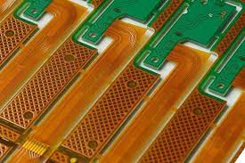
A flex pcb fabrication flexible section can be made up of different layers depending on the specific application it will be used in. The flex layer’s thickness should be set based on the bending radius required by the final application. For example, a tighter bending radius may require thinner copper layers. A smaller thickness will also mean less flexibility.
The flex layer can be reinforced with stiffeners for additional mechanical stability. Stiffeners are usually made of FR-4 or metal and help to prevent the rigid sections from warping during lamination. The flex and rigid section’s layers can be laminated to each other using a conductive epoxy or thermally stable adhesive.
How to Ensure Dimensional Accuracy in Flex PCB Fabrication
A flex circuit board’s rigid section can also have holes drilled through it to allow for soldering of components. However, this can cause stress on the copper traces and could lead to a cracking of the traces during bending. To avoid this, it’s recommended to stagger vias when building a flex circuit. This will reduce the amount of force applied to the traces by evenly spreading the pressure across the entire pad.
Rigid-flex boards are prone to warping due to the differences in the thermal expansion coefficients of the material that make up the flex and rigid-flex sections of the circuit board. This can impact the accuracy of the dimensional tolerances and the adhesion between the layers after the board has been pressed together. To combat this, the flex circuit board maker should have a robust quality control system in place that includes first-article inspections, in-process checks, end-product testing, etc.
Getting the right material layup is critical for a flex-rigid PCB to ensure performance, reliability, and cost. This requires close collaboration between the designer and the flex-rigid manufacturer to get the best possible result.
For example, reducing the number of layers and minimizing the size of the traces will help to minimize cost while maintaining the dimensional accuracy needed for the design to function properly. It’s also recommended to offset conductors rather than making them parallel as this will decrease the chances of them cracking during bending. Lastly, avoiding placing the shortest tracks at the edge of the flex section will further prevent traces from being damaged by mechanical stress. This is especially helpful in harsh environments like military and aerospace applications where a flex-rigid circuit board needs to withstand extreme temperatures and vibrations.